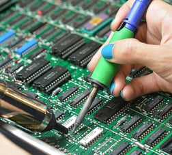
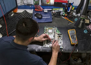
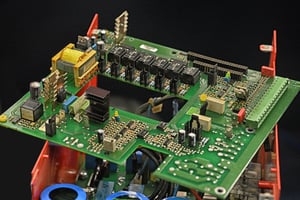
 The printed circuit board was introduced to us nearly 90 years ago, and along the way, it has seen massive improvements. As technology has progressed and evolved, these boards have continued to become more sophisticated. A printed circuit board or a PCB connects electrical components by conductive paths or tracks that have been printed or etched on the board. Check out more about What a Printed Circuit Board Is and what it is used for here.
Historical Background:
Today PCBs are a vital component in our electronic devices. Before the appearance of these boards, we were met with bulky and impractical designs that were unreliable in electronics. Printed circuit boards continue to expand in capabilities and power, while simultaneously decreasing in size. The invention of the printed circuit board has undergone mass enhancements and has been through an array of constant improvements throughout its evolution.
In 1927, Charles Ducas submitted a patent for a “Printed Wire.” However, the actual start of this circuit came in 1943 by an Austrian engineer. While working in England, Dr. Paul Eisler made the first working Printed Circuit Board. His invention caught the eyes of the American and British Military. The U.S Department of Defense understood they needed a new approach for communication during the War. They were then able to use this technology during WWII to improve radios and weaponry.
The Military was also able to ramp up production of the printed circuit board by utilizing auto assembly. Much of the acknowledgment to the rise of this technology is credited to the U.S Military. They made the construction of these boards quicker, which allowed them to take over as the main component in electronic devices.
 Timeline/Evolution:
In 1948 after WWII this technology was released for commercial use. Printed circuit board use grew in the 1950s when PCBs were used in most electronics rather than their bulky wiring counterpart. Despite that fact, they were still limited to only one side. It was not until the U.S Patent office allowed a scientist from the United States Army to move forward with the “Process of Assembling Electrical Circuits,” that this changed. This led to immense innovations for printed circuit boards.
By the 1960s, multilayer printed boards were being assembled. While small devices could function with just one board, larger devices needed one or more of these boards. By the 1970s, the size and circuity of these circuits were becoming much smaller than ever before. Alongside this, hot air soldering and surface mounting were now the preferred choices over the older through-hole components. These improvements created efficiency and allowed for the board to handle greater demands. Surface mounting technology or SMT is used over wiring, which are small components that are attached directly to the board. This upgrade allowed soldering to be utilized and automated production, which overall increased dependability. Components are now able to be soldered into the formation of the board.
 The United States was also able to use this technology in space exploration. PCBs allowed for increased efficacy for spaceships due to its lightweight and low electricity use even when performing complex tasks. NASA used PCBs during its Apollo program in 1969, which eventually helped land man on the moon. Stemming from this, modern PCB technology now helps new space ventures take flight. With its start in 2002 SpaceX is a space venture that is utilizing these powerful and flexible boards to make their systems possible. The future for PCBs inside space exploration is undoubtedly going to be a remarkable one to watch.
By the 80s and 90s, the modernized printed circuit board was rising and advancing more than ever. Multilayer PCB assemblies were constructed which allowed circuits to be connected. These layers allowed for a smaller and even more flexible board. By the mid-90s production for U.S printed circuit boards reached 7 billion and by the early 2000s, it reached 10 billion. In this internet era, PCBs made computers smaller and gave significant enhancements to cellphones as well as making cellular antennas obsolete. Even though these boards have become far more advanced since their infancy, they continue to decrease in size and cost.
Future of PCBs
Today, the complexity of these board is far more advanced than at the start of their use. Technology is always changing and becoming increasingly better. The PCB is continuously becoming more efficient to meet the demands of that ever-changing technology. With the rise of “miniaturization,” smaller and more compact PCBs are being strived towards. In the near and far future, we will likely see even better incarnations as these boards adjust and change to keep up with technology. Looking back to the invention of printed circuit boards, it’s incredible to see how they have developed over time.
To learn more about Radwell International

